Measuring modes:
- AFM/ LFM/ ResonantMode/ Phase Imaging/ Local elasticity/ MFM/ EFM/ SCM/ Spreading Resistance Imaging/ Adhesion Force Imaging
Noise level: <1 Angstrom RMS in vertical (Z) direction
SPM configuration:
- 30x30x1.5um or up to 100x100x5um scanner
- Residual lateral nonlinearity (in XY - direction) less than 1%
- Advanced electronics High-Q (22 bits XY resolution) allows to set the resonance frequency with an accuracy 0.01 Hz
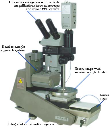
Sample size:
- Up to 250mm (300mm optional) in diameter
- Up to 15mm thick
Sample holder:
- Vacuum chuck for CD stampers, replicas and glass master discs
- Vacuum chuck for hard discs (48mm, 65mm, 95mm, and 130mm) and other samples
- Semiconductor wafer vacuum chuck for 50mm, 100mm,125mm, 150mm, 200mm and 250mm wafers
Motorized Positioner:
- Inspectable area up to 250mm in diameter with linear and rotary stage
- Linear resolution — 2um
- Bidirectional repeatability — 1um
- Angular Resolution 0.002 degree
- Angular Repeatability 0.0014 degree
Environmental conditions:
- temperature - 25+/-15 °C
- humidity - 80%
Optical microscope:
- Resolution 5um (with optional objective — up to 1.5um)
- Field of view
- with 14X eyepieces: 2.4mm to 28mm
- Magnification
- with 14X eyepieces: 8.4X to 100X
- with color CCD: 43X to 470X
Tip Viewing: Scanning cantilever can be viewed on the monitor screen during scanning procedure
Preview: Surface defects can be located during whole wafer preview operation with 8X eyepieces (field of view 39mm). The cantilever can be positioned on the predefined area for further scanning. |